The MOTOROLA MC100ES6226 is a bipolar monolithic differential clock distributed buffer and clock divider. Designed for the most demanding clock distribution systems, the MC100ES6226 supports a variety of applications that require large volumes of output to drive precisely aligned clock signals.
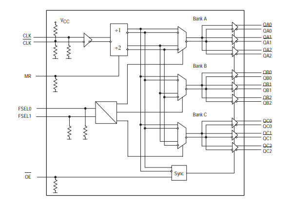
Logic Diagram
The device uses SiGe technology and a fully differential architecture, providing superior digital signal characteristics and very low clock tilt error. The target applications of this clock driver are high performance clock distribution systems for computing, networking and telecommunications systems
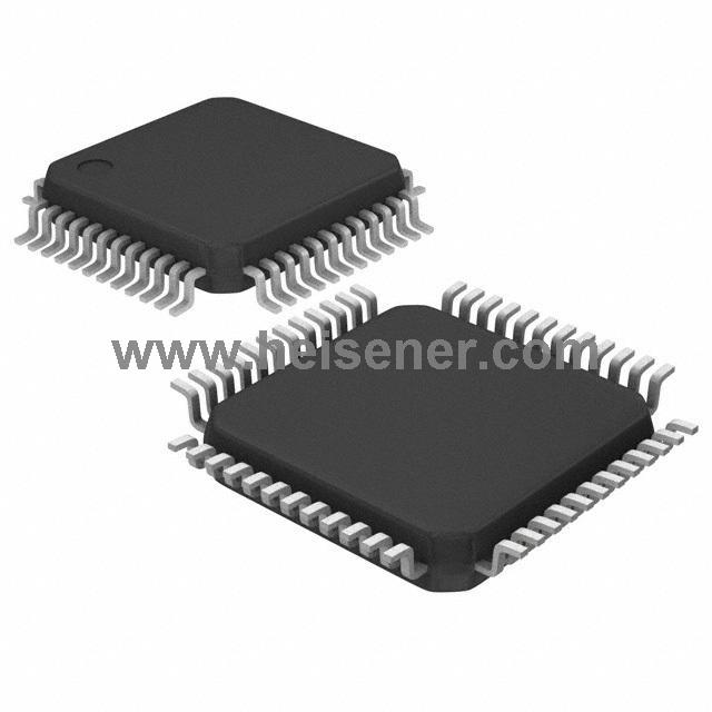
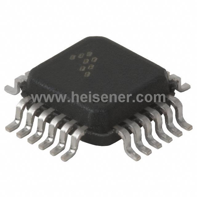
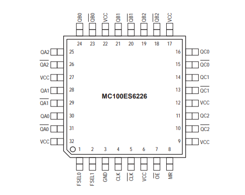
32 -- Lead Package Pinout (Top View)
Functional Description
Designed for extremely skewed critical differential clock distribution systems, the MC100ES6226 supports clock frequencies from DC to 3.0 GHz. Typical applications of the MC100ES6226 are master clock distribution systems on backplanes for high performance computers, networking and telecommunications systems, and on-board clocks for OC-3, OC-12, and OC-48 speed communication systems.
The MC100ES6226 can operate on a 3.3V or 2.5V positive power supply and does not require a negative power supply. Each output group of the three differential clock output pairs can be configured independently to assign input frequency or half of the input frequency. The FSEL0 and FSEL1 clock frequency selections are asynchronous control inputs. Any change in the control input will require an MR Pulse to resynchronize the ÷2 output.
Features
● Fully differential architecture from input to all outputs
● SiGe technology supports near-zero output skew
● Selectable 1:1 or 1:2 frequency outputs
● LVPECL compatible differential clock inputs and outputs
● LVCMOS compatible control inputs
● Single 3.3V or 2.5V supply
● Max.35 ps maximum output skew (within output bank)
● Max. 50 ps maximum device skew
● Supports DC operation and up to 3 GHz (typ.) clock signals
● Synchronous output enable eliminating output runt pulse generation and metastability
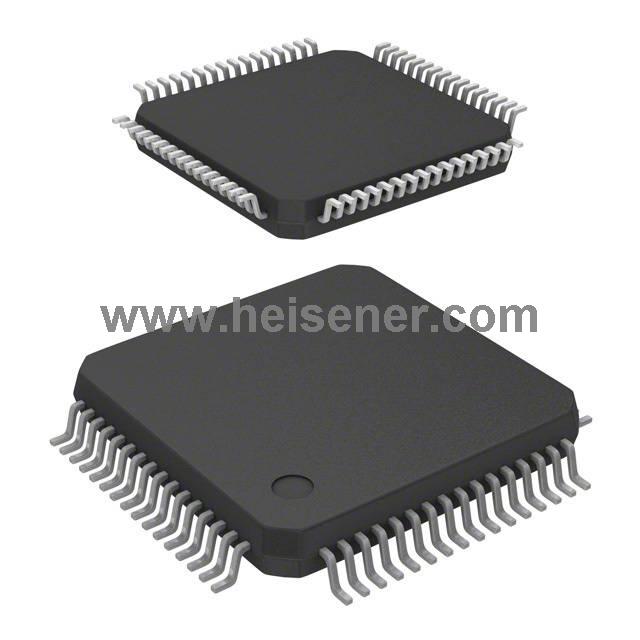
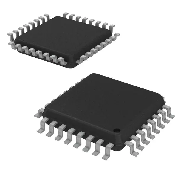
● Standard 32 lead LQFP package
● Industrial temperature range
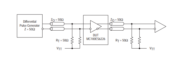
MC100ES6226 AC test reference