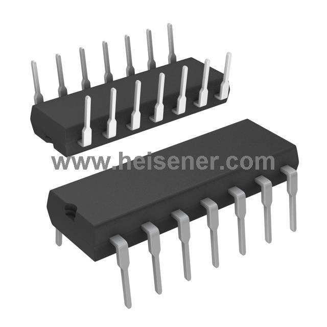
LM2907N Introduction
The LM2907N is a frequency-to-voltage converter that transforms an input frequency into a proportional voltage. It features a high-gain op-amp and is used in applications like controlling relays, lamps, or other loads when a frequency threshold is reached. Using a charge pump technique with frequency doubling and low ripple, it provides stable output.
This 8-pin device drives loads up to 50mA with a floating transistor output. Its output swings to ground for zero frequency input, and the collector can go up to 28V above VCC. The LM2907N is ideal for frequency-to-voltage conversion, with a ground-referenced tachometer input for easy system integration.
LM2907N Functional Block Diagram

LM2907N Pinout

COL: The collector of the bipolar junction transistor
CP1: A capacitor placed on this pin will be charged up to VCC/2 by a constant current source of 180 μA typical at the start of every positive half cycle. At the beginning of negative half cycles, this capacitor is discharged the same amount at the same rate.
CP2: The charge pump sources current out of this pin equal to the absolute value of the capacitor current on CP1. A resistor and capacitor in parallel connected to this pin filters the current pulses into the output voltage.
EMIT: The emitter of the bipolar junction transistor
GND: Ground
IN+: The noninverting input to the high gain op amp
IN–: The inverting input to the high gain op amp
NC: No connect
TACH+: Positive terminal for the input signal that leads to the noninverting terminal of the internal Schmitt-Trigger comparator.
TACH–: Negative terminal for the input signal that leads to the noninverting terminal of the internal Schmitt-Trigger comparator.
V+: Supply voltage
LM2907N Test Circuit

LM2907N Tachometer Diagram

LM2907N Specification
| Specification | Details |
| Frequency | 10 kHz |
| Linearity | ±0.3% |
| Output Load Current | Up to 50 mA |
| Input Voltage (VCC) | 3V-40V |
| Maximum VCE (Collector-Emitter Voltage) | 28V |
| Op-Amp Type | High-Gain Operational Amplifier |
| Power Supply Current | 2.5 mA |
| Frequency Doubling | Yes, with low ripple |
| Tachometer Input | Ground-Referenced |
| Applications | Relay control, lamp drive, frequency switching, tachometers |
| Temperature Range | -40°C~85°C |
| Package | 14-PDIP |
LM2907N Features
Ground Referenced Tachometer Input Interfaces
Directly With Variable Reluctance Magnetic Pickups
Op Amp Has Floating Transistor Output
50-mA Sink or Source to Operate Relays, Solenoids, Meters, or LEDs
Frequency Doubling For Low Ripple
Tachometer Has Built-In Hysteresis With Either Differential Input or Ground Referenced Input
±0.3% Linearity (Typical)
Ground-Referenced Tachometer is Fully Protected From Damage Due to Swings Above VCC and Below Ground
Output Swings to Ground For Zero Frequency Input
Easy to Use; VOUT = fIN × VCC × R1 × C1
Zener Regulator on Chip allows Accurate and Stable Frequency to Voltage or Current Conversion (LM2917)
LM2907N Applications
Over- and Under-Speed Sensing
Frequency-to-Voltage Conversion (Tachometer)
Speedometers
Breaker Point Dwell Meters
Hand-Held Tachometers
Speed Governors
Cruise Control
Automotive Door Lock Control
Clutch Control
Horn Control
Touch or Sound Switches
LM2907N Package
The LM2907N comes in a 14-PDIP package, suitable for applications that require frequency-to-voltage conversion. This package offers ample space, making it easy to mount on a PCB with through-hole installation, ideal for applications where space constraints are not critical.

How to Connect LM2907N?
First, make sure to connect the V+ pin to the positive terminal of the power supply, typically +VCC, and the GND pin to the negative terminal of the power supply, serving as the ground. Next, connect the input signal to the TACH+ and TACH- pins, which correspond to the positive and negative terminals of the input signal. These pins process the input signal via the internal Schmitt trigger.
Then, the CP1 pin should be connected to a capacitor that will charge up to VCC/2, with a current source of 180μA typically providing the current during each positive half-cycle. The CP2 pin requires a parallel resistor and capacitor to filter the current pulses coming from CP1, converting them into the output voltage.
Next, connect the COL pin to the positive terminal of the load, and the other side of the load to the EMIT pin. Since the LM2907N’s output is floating, this will allow it to drive the required load, with a maximum current of 50mA.
Finally, connect the IN+ and IN- pins to the non-inverting and inverting inputs of the high-gain operational amplifier, respectively, to process the gain of the input signal. If certain function pins, such as NC (no connection), are not being used, they can remain unconnected and left open.
FAQs
What is the LM2907N?
The LM2907N is a monolithic frequency-to-voltage converter that converts an input frequency signal into a corresponding output voltage. It includes a high-gain operational amplifier and a charge pump circuit for stable output with low ripples. The device is ideal for applications requiring frequency detection and control, such as operating relays, lamps, or other loads based on the input frequency.
How does the LM2907N handle zero-frequency input?
When the input frequency is zero, the output of the LM2907N swings to ground. This provides a clear indication of no frequency input, making it easy to detect and process low or zero-frequency signals.
What is the maximum load current the LM2907N can drive?
The LM2907N can drive loads up to 50mA. The load is driven through the COL pin, which is the collector of the internal transistor, and the EMIT pin, which is the emitter.