The current in an electronic circuit usually has to be limited. In USB ports, for example, excessive current must be prevented to provide reliable protection for the circuit. Also in the power bank, the battery must be prevented from discharging. Too high discharge current results in too large voltage drop of the battery and insufficient supply voltage of downstream devices.
Therefore, it is often necessary to limit the current to a specific value. Most power converters have an overcurrent limiter to protect them from damage caused by extra current. In some DC-DC converters, you can even adjust the threshold.
Figure 1:Each port output current is 1 A power bank current limit

In Figure 1, you can also use a DC-DC boost converter with a built-in or even adjustable current limiter. In this case, no additional current limiter module is required. However, there are also many applications that do not use a DC-DC converter in the power channel. For example, when the voltage in the system is 24 V, the current in the line should be limited, but the load must operate at exactly 24 V. In this case, an additional current limiter module can be used, as shown in blue in Figure 1.
The current limiter circuit provides a solution to this problem. It comes from a family of protection modules, including hot swap controllers, surge protectors, electronic circuit protectors and ideal diodes.
Most ics on the market use an external MOSFETs as switches to turn current on and off, as well as to limit current, in which case the switch works in a similar way to a linear voltage regulator. However, this switch must ensure that the MOSFET is always operating within its secure workspace (SOA). Otherwise, semiconductors and circuits will be damaged. Unfortunately, picking the right MOSFeTs and running them in a way that never crosses SOA is sometimes not easy. Operating temperature, voltage, current, and especially time will affect it. To ensure safe operation, you must carefully consider these factors and make the right choice. Figure 2 shows the SOA diagram for a typical n-channel MOSFETs. Allow the MOSFET to run under the shown line.
Figure 2. Typical SOA for MOSFET

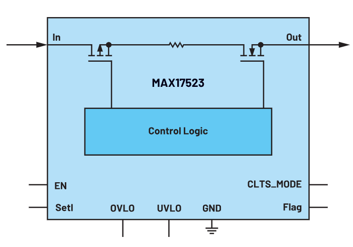
Figure 3 shows a dedicated current limiter IC -- ADI's MAX17523. It has two MosFeTs that can limit the current to some value between 150 mA and 1 A. If the current reaches the limit, the current is cut off and waits for a period of time before resuming, or the current continues to be interrupted until the next turn on, or the current is limited by lowering the voltage. The internal mosFeTs then operate in the ohmic region. This is a linear voltage regulator function. In these adjustable limiting modes, the internal MOSFETs are always located within the SOA and are not compromised. No detailed calculations or evaluations are required.
Figure 3. Simplified circuit diagram of special current limiter IC

Limiting the current in the circuit is not a problem if a suitable highly integrated IC is used. It is also possible to combine this type of circuit with a DC-DC converter without an adjustable current limiter.
Traction inverters are the main battery drain components in electric vehicles (EVs), with power levels up to 150kW or higher. The efficiency and performance of traction inverter directly affect the driving range of electric vehicle after a single charge. Therefore, in order to build the next generation of traction inverter systems, silicon carbide (SiC) field effect transistor (FET) is widely used in the industry to achieve higher reliability, efficiency and power density.
Do you know the 8 application circuits of operational amplifiers?
This technical presentation requires an understanding of how to configure an operational amplifier in a typical gain control circuit. The applications of linear and nonlinear digital potentiometers are discussed. This article gives an overview of the basic techniques required to convert audio and other potentiometer/op amp applications from conventional mechanical potentiometers to solid state potentiometers
The current in an electronic circuit usually has to be limited. In USB ports, for example, excessive current must be prevented to provide reliable protection for the circuit. Also in the power bank, the battery must be prevented from discharging. Too high discharge current results in too large voltage drop of the battery and insufficient supply voltage of downstream devices
Using advanced real-time control technologies such as motor control circuits with higher power density, higher integration and more efficient systems, better acoustic performance of the system can be achieved
Brushless direct current (BLDC) motors have been widely used in household appliances, industrial equipment and automobiles. While brushless DC motors offer a more reliable and maintainable alternative to traditional brushless motors, they require more sophisticated electronics to drive them
How to achieve precise motion control in industrial actuators
The NCP51820 is a 650 V, high-speed, half-bridge driver capable of driving gallium nitride (" GaN ") power switches at dV/dt rates up to 200 V/ns. The full performance advantages of high voltage, high frequency and fast dV/dt edge rate switches can only be realized if the printed circuit board (PCB) can be properly designed to support this power switch. This paper will briefly introduce NCP51820 and the key points of PCB design of high performance GaN half bridge grid driver circuit using NCP51820